
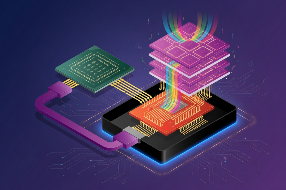
NVIDIA has expanded NVLink Fusion with NVHBM, a custom high bandwidth memory technology that relocates the memory controller from the processor die into the HBM base die itself, and the architectural detail matters less than the territorial one: NVIDIA is now designing the silicon that sits inside other companies' memory stacks.
Read the announcement's numbers first. By integrating its custom memory controller into the 3D HBM stack instead of the XPU, NVIDIA says NVHBM delivers up to 30 percent greater memory bandwidth and 15 percent lower HBM power consumption while freeing up to 25 percent more area on the compute die, all compared with standard HBM4E. Those are NVIDIA's own figures from its announcement blog, with no benchmark methodology attached yet, and the appropriate posture toward them is the usual one: plausible, unverified, vendor supplied.
Decode the structure and the strategy is plain. The memory controller has historically been the processor designer's silicon, sitting on the XPU and consuming die area that could be compute. Moving it into the base die means every NVHBM stack ships with NVIDIA's controller inside, validated and offered by what the company calls leading memory partners. NVIDIA says it is establishing a standard NVHBM implementation available from multiple providers, which reduces qualification work for customers building custom chips. It also means the memory makers manufacture a product with NVIDIA's design at its heart, for customers building processors that compete with NVIDIA's own.
Amazon is the proof the offer works. Annapurna Labs, Amazon's chip division, will be the first partner on NVHBM as part of its NVLink Fusion collaboration, and its next generation Trainium4 accelerators will support NVLink Fusion, letting Amazon silicon and NVIDIA GPUs share a rack scale architecture. Annapurna's vice president Nafea Bshara called the technology a new architectural approach to memory performance in the announcement, and the willingness of the industry's most credible custom silicon operation to adopt a rival's memory controller says more than the press release language does.
Set this beside the week's other memory news and a pattern emerges. SK hynix spent Hot Chips explaining the physical ceilings closing in on HBM stacks, Samsung is pushing logic into the base die of its own HBM, and now NVIDIA claims the base die for itself across the whole NVLink Fusion ecosystem. The base die is becoming the most contested few square millimeters in computing, because whoever owns it owns the interface between memory and everything else.
Bootnote: the phrase NVIDIA uses for NVLink Fusion is vertically integrated and horizontally open, which is a genuinely elegant way to describe giving everyone access to a road you own. The last company to run that playbook at the interface layer was Intel with the PC chipset, and it worked for twenty five years.



Leave a Reply