
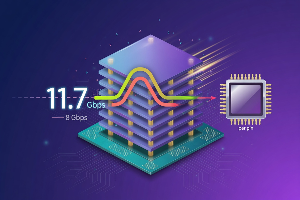
Samsung has begun mass production of HBM4 and shipped commercial parts to customers, and the figure the company set beside that announcement is the one worth reading twice. It rates the memory at a consistent 11.7 gigabits per second on every pin, against an industry standard of 8.
HBM stands for high bandwidth memory, said letter by letter, and the idea underneath it is less exotic than the marketing around it. The trick is to stack the memory dies vertically, sit the stack right next to the processor, and drill connections straight down through the silicon so the trip is short. Picture the link between stack and processor as a loading bay. HBM4 doubles the number of doors from 1,024 to 2,048.
Width is only half the story. Speed per pin is the other half, and 11.7Gbps works out to roughly 46 percent above that 8Gbps baseline and 1.22 times the 9.6Gbps peak pin speed of HBM3E, the generation being replaced. The release adds that performance can be pushed as far as 13Gbps.
That ceiling matters once the bandwidth headline arrives. Samsung gives a maximum of 3.3 terabytes per second per stack, and 2.7 times HBM3E. Run the arithmetic across 2,048 pins and the 3.3 figure lands on the 13Gbps ceiling rather than on the 11.7Gbps the company describes as consistent, where the same stack comes out nearer 3 terabytes per second. Spec sheets like to quote the brave number in one line and the safe number in another, a habit that has cost me money at least once.
The engineering bet sits underneath all of it. Rather than reuse an older and well understood process, the memory core is built on a sixth-generation 10nm-class DRAM node the company calls 1c, and the logic base die at the bottom of the stack is made on a 4nm process.
"Instead of taking the conventional path of utilizing existing proven designs, Samsung took the leap and adopted the most advanced nodes like the 1c DRAM and 4nm logic process for HBM4," said Sang Joon Hwang, Executive Vice President and Head of Memory Development at Samsung Electronics.
Doubling the input and output count is a heat problem as much as a bandwidth one, and the answering claims are specific. Against HBM3E, Samsung reports a 40 percent gain in power efficiency from low-voltage through-silicon vias and a reworked power distribution network, a 10 percent improvement in thermal resistance, and 30 percent better heat dissipation. Each of those figures is measured against the previous generation, not against a competing part.
Capacities run from 24 to 36 gigabytes on 12-layer stacks. A 16-layer version would reach 48 gigabytes, which the company says it will keep aligned with customer timelines rather than commit to a date of its own.
Commercially, the ambition is stated plainly. Samsung anticipates HBM sales more than tripling in 2026 against 2025 and says it is expanding HBM4 capacity accordingly, with HBM4E sampling expected to start in the second half of the year and custom HBM samples reaching customers in 2027.
One claim in the release carries no number, and it is the one that decides whether the rest holds. Samsung says it reached stable yields from the outset of mass production without additional redesigns. Yield is the figure memory makers disclose least and customers discover first, and no independent measurement of it exists yet.




Leave a Reply