
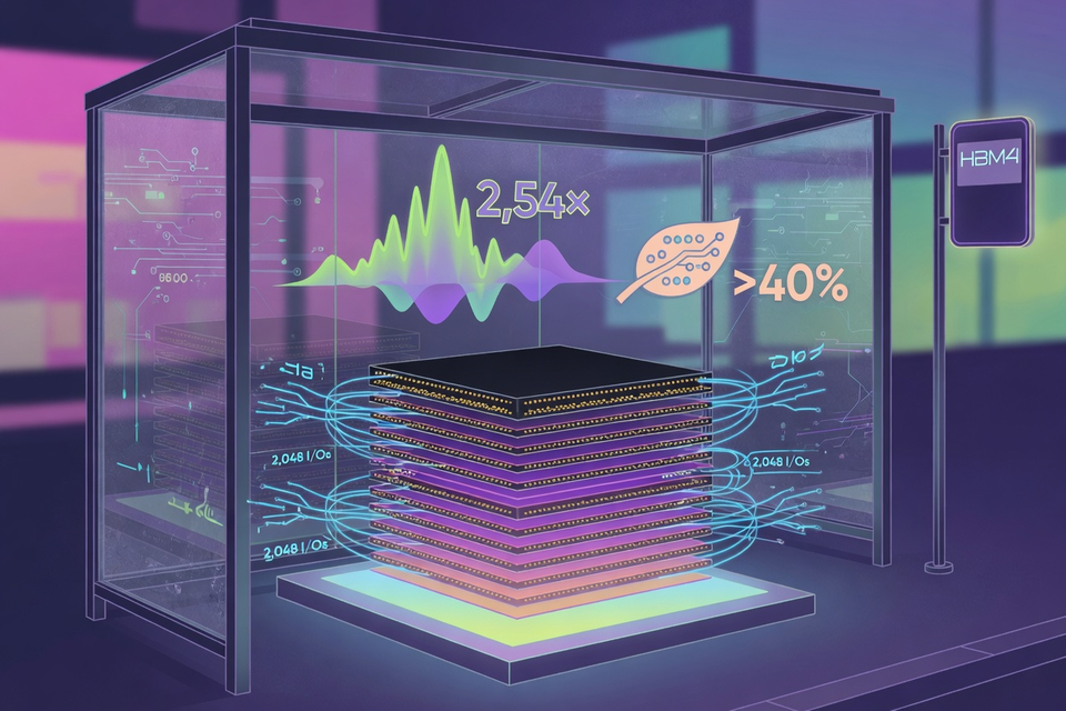
SK hynix put HBM4 on show at Mobile World Congress 2026 with 2,048 I/Os, a claimed 2.54 times the bandwidth of the previous generation and a power efficiency gain of more than 40 percent, and published no absolute figure for any of it.
The release states that HBM4 "delivers 2.54 times the bandwidth of the previous generation and improves power efficiency by more than 40%". Both numbers are ratios. Neither has a denominator on the page.
Work out what the baseline is and the company's own footnotes do the job. The glossary attached to the release defines six HBM generations ending "HBM3E, and HBM4", so the previous generation is HBM3E. Which HBM3E is not stated. The part on the stand is the 12-layer version, and SK hynix says that one is already in AI data centre GPU modules at global customers.
The I/O count is the one hard specification in the paragraph, and it carries most of the multiplier. If the comparison is against a 1,024-bit HBM3E stack, doubling the interface width to 2,048 accounts for 2x on its own. Dividing 2.54 by 2 leaves 1.27, so the remaining 27 percent has to come from per-pin signalling rate. That rate is what a system architect sizes a design around, and it is what the release omits.
Power is looser still. More than 40 percent better efficiency arrives with no unit, no capacity point, no workload and no measurement method. Picojoules per bit, watts at fixed bandwidth and watts at fixed capacity are three different claims, and the release picks none of them.
Precision is clearly available when the company wants it. In the data centre zone it named DDR5 RDIMM at 64GB on what it calls the world's first 10-nanometer sixth-generation process, a 3DS DDR5 RDIMM at 256GB, an MRDIMM at 96GB and SOCAMM2 at 192GB. The enterprise SSD line got model numbers and form factors, including a PEB210 E1.S in a 9.5mm chassis supporting direct liquid cooling and a QLC-based PS1101 E3.S reaching 122TB. On the mobile side, uMCP 4.1 was specified down to its contents, 16GB of LPDDR5X and 512GB of UFS in one package.
LPDDR6 got none of that. It appeared as the newest member of the LPDDR family with no speed grade, no density and no availability, alongside an automotive LPDDR6 built on the same 1c process. For a part whose entire commercial argument is bandwidth per milliwatt, showing it without a data rate is a decision rather than an oversight.
That pattern holds across the release. Where a product is already shipping into a known socket, the numbers are concrete. Where it is a flagship still moving through customer qualification, the claim converts to a ratio and the baseline goes unstated. The only quotation in the whole release is attributed to "A representative of SK hynix" and names no one, which tells its own story about how much the company wanted pinned to any of this.
Bootnote: the six-generation HBM count in that glossary is worth keeping. Vendors periodically renumber the family, and having the issuer commit in writing that HBM4 follows HBM3E is what makes the 2.54x claim resolvable at all.




Leave a Reply