
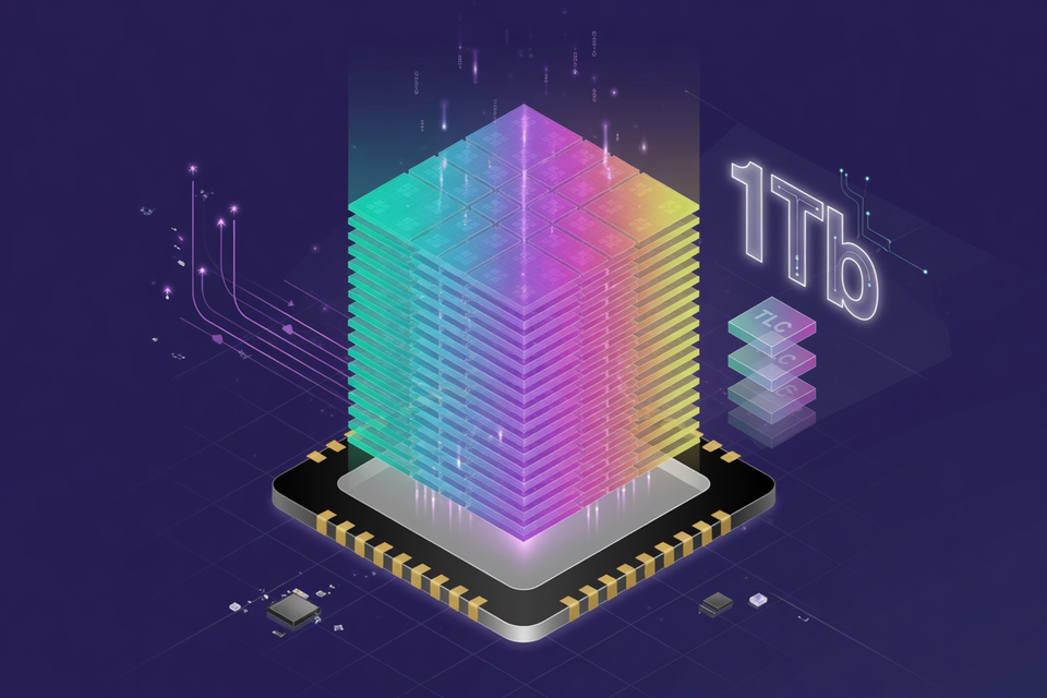
Sandisk and Kioxia have begun sampling BiCS10, the tenth generation of the 3D NAND they jointly develop, at 332 layers and 1Tb per die in TLC.
Each company issued its own announcement for the same silicon, and the figures they agree on are the ones that matter. Sandisk puts 1Tb TLC memory density above 29Gb/mm2, a 59 percent bit density improvement, with interface speed up to 4.8Gb/s, a 33 percent gain on the eighth generation now in mass production. Kioxia states the same 59 percent and the same 4.8 Gb/s.
"As the world becomes more connected, data-intensive and intelligent, NAND plays an increasingly mission-critical role in delivering the performance, efficiency and scale modern computing requires," said Alper Ilkbahar, CTO at Sandisk.
Decoded, that is a claim about cost per bit, and the interesting detail is where the 59 percent came from. Kioxia attributes it to stacking 332 layers and improving lateral density, and Sandisk credits advanced lateral scaling techniques for its density figure. Neither company presents the gain as stacking alone. That matters, because vertical stacking is the expensive half of the equation in etch time and yield, and any bit density a vendor can win laterally is cheaper to produce.
Power is where the two partners stop agreeing, and the disagreement is instructive. Sandisk reports a 10 percent reduction in data input power and 34 percent in data output power against BiCS8. Kioxia reports write and read power efficiencies improved by 18 percent and 30 percent. Same joint venture wafers, two different measurement frames, and neither release publishes its test conditions. Kioxia's own footnote states that its values were obtained in a specific test environment at Kioxia and may vary depending on use conditions. Take the direction rather than the decimal.
Production is planned at Kitakami Plant Fab2 in Iwate Prefecture, Japan, according to Kioxia, and neither company has attached a mass production date or named a first commercial product. Both stress that samples are for functional evaluation and that specifications may differ in mass production, which is standard language and should be read as written rather than as a schedule.
Competitively the position is narrower than the layer count suggests. StorageReview places BiCS10 in the same class as SK hynix's 321-layer generation, and Blocks and Files reports Samsung at 400 layers on its tenth generation V NAND. On that reading 332 buys parity rather than a lead, and what Sandisk and Kioxia actually hold is process: CBA, which builds the CMOS logic and the memory array on separate wafers and bonds them, paired with On-Pitch Select Gate Drain, which recovers area by removing unused memory holes. Both were adopted at the eighth generation, so BiCS10 scales a known process rather than introducing one.
Interface speed is what SSD controller vendors will price first. At 4.8Gb/s, BiCS10 offers the NAND side bandwidth that PCIe Gen6 class drives need, which is precisely the enterprise and data center demand Kioxia says it is aiming the parts at.
Bootnote. There is a ninth generation, and its absence from this announcement is deliberate. Kioxia describes a dual-axis strategy, running its ninth generation for high performance at relatively low cost of investing alongside a tenth generation that leans on layer stacking for capacity. Two roadmaps, one fab, and a customer base that will pay for different things.


Leave a Reply