
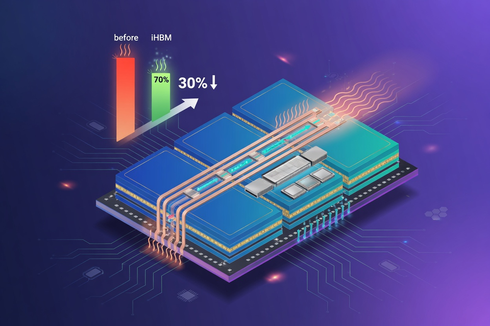
SK hynix has decided that the best place to fight heat is the exact spot where it is made. The company, SK hynix, has announced a packaging design called iHBM that embeds cooling elements inside the high bandwidth memory package itself, and it puts the improvement at a 30 percent reduction in thermal resistance.
High bandwidth memory, which almost everyone pronounces letter by letter as H-B-M, gets its speed by stacking DRAM dies straight up beside the processor instead of spreading them across a board. Picture a dense city block rather than a sprawl of suburbs. The commute for each bit is short, which is the entire point, and the drawback is that everything runs hot in a very small footprint.
Most of that heat collects in one neighborhood. The die to die physical layer, mercifully shortened to D2D PHY, is the hardware interface that moves data between the HBM base die and the AI accelerator sitting alongside it. SK hynix describes the amount of heat produced per unit of space there as a factor that defines how competitive a next generation HBM part will be, which is easy enough to believe given how many lanes are switching at once inside an area that small.
Conventional packages handle this indirectly. They draw heat away through the core die and let the surrounding structure disperse it, an arrangement that works until the concentration outruns the path available to it. iHBM instead places what the company calls integrated cooling elements, or ICEs, directly in the D2D PHY area where the concentration is worst. The company describes them as a silicon based material that conducts heat well while not conducting electricity, a distinction that matters enormously when the thing being cooled is a dense field of high speed signalling lanes. The result is an additional route for heat to leave by, and SK hynix says chips can then hold stable operation in high temperature and high pressure conditions.
Volume manufacturing is usually where clever packaging ideas go to die. The company says this one can be produced through its wafer level packaging process, which is built on the mass reflow molded underfill technique already running in its commercial HBM products. It also says the design keeps a high degree of compatibility with existing system in package layouts, so a customer would face minimal design adjustments to take it on.
Timing is looser. SK hynix says iHBM is slated for next generation products including HBM5, and it has not said where that list ends. The stated aim is to improve stability and operating efficiency in high performance computing and in AI data centers, which are precisely the places where density and bandwidth are both being pushed hardest.
Kangwook Lee, the company's senior vice president and head of PKG development, framed the technology as its memory design work and its advanced packaging arriving together in one part, and said the company would move early to offer what customers need in AI environments and hold its lead in AI memory.
Whether 30 percent turns out to be the number that matters will depend on what HBM5 stacks actually demand once they exist, and that is a question the packaging roadmap has not answered yet.


Leave a Reply