
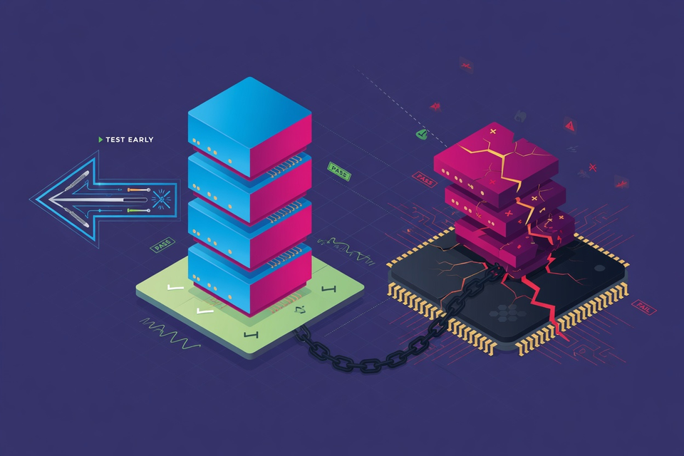
When a GPU fails inside an AI data center, the memory bolted alongside it is the prime suspect. “Data from hyperscalers indicates that HBM failures are the number one cause of GPU failures in data centers,” Faisal Goriawalla, director of product management at Synopsys, tells Semiconductor Engineering. One obscure corner of chip manufacturing, the order in which things get tested, has turned into an expensive argument as a result.
HBM, pronounced letter by letter, is high bandwidth memory, and the whole idea is geometry. Picture a dozen wafer-thin silicon pancakes stacked flat and skewered by thousands of microscopic straws, so data climbs the pile instead of trekking across the circuit board. Those straws are through-silicon vias, and lining them up with the bumps underneath is work measured in microns. Stacks have grown from two dies to twelve over the past decade, sixteen is expected next, and a single AI assembly now carries eight stacks where it once carried four.
Semiconductor Engineering reports that HBM accounts for nearly half the cost of AI chips. Find a dead stack at final test and the money is already spent, which is why the industry has fixed on the idea of a known good stack, meaning one proven sound before anything expensive is glued to it. “It all comes down to cost,” says Vernon Rodgers, executive vice president of sales and marketing at Aehr Test Systems.
The multiplier is what stings. Under every HBM tower sits a logic base die, and it provides the only electrical route into the memory above it. Rodgers does the arithmetic. “Making sure that base logic device is of the highest quality is critical, because if it’s bad, 16 dies get thrown away. So it’s a huge multiplier in the yield curve.”
Shifting test left means moving those insertions earlier, into wafer-level burn-in, hot and cold testing and repair, before dies are ever thinned, bumped and stacked. Kevin Tran, senior director of product marketing at FormFactor, sets out the payoff. “This shift left helps prevent defective dies from entering expensive stacking processes and drives increased use of high‑speed test, wider parallelism, and tighter thermal control at wafer test.”
Heat is the awkward part of all this, because a tall stack cools from its skin inward and the middle floors have nowhere to send their warmth. “If you look at a 16-story building, the sun hits the outside and the center doesn’t really get the heat,” Rodgers says. “It’s the reverse in a stacked die. The outside is cooled, but how do you get the heat out of the center?”
Who is leaning on the memory makers is not a mystery either. Hanh Lai, product marketing manager in the memory division at Teradyne, points at the companies buying the finished packages. “The reason is that integrators (i.e., Nvidia and AMD) are concerned about final package yield. In the typical GPU package, a GPU is surrounded by eight HBM stacks. One defective HBM stack becomes very costly at that particular point.”
None of this comes cheap. Every extra insertion adds test time, and the step several vendors would most like to have, testing a stack after it has been cut free of the wafer, is not done in production today. Prober companies are working on it. Semiconductor Engineering describes the economic impact as unknown, and unknown is doing a great deal of work in that sentence.



Leave a Reply