
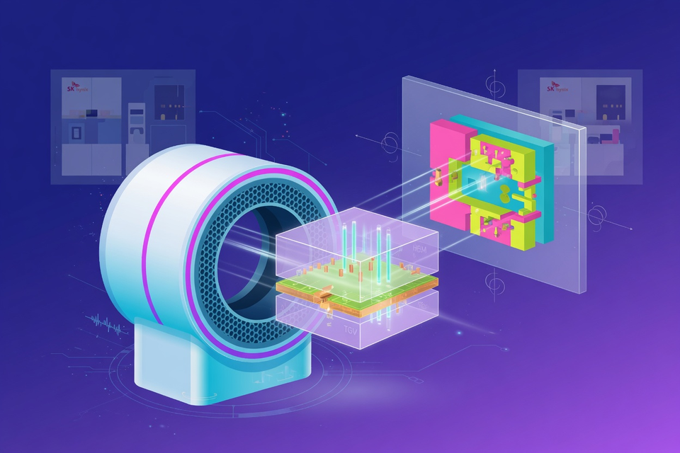
Korean X-ray inspection vendor Techvalley has delivered one 3D computed tomography system each to Samsung Electronics and SK hynix for in-house research and development on high bandwidth memory and through-glass vias.
The Elec reports the deliveries citing industry sources, and neither memory maker has confirmed them. The tools are customized builds of Techvalley's Teraton line rather than catalogue units, with changes to rotation axes, table size and software to suit each customer's inspection requirements. The standard model is priced at around 1 billion won, and the custom versions are expected to cost more.
Both Teraton 5 and Teraton 7 use high-resolution X-ray tubes running at 160 kilovolts. The Elec puts the Teraton 5 at 64 watts and the Teraton 7 at 16.6 watts, with the higher-power unit inspecting faster and the lower-power unit resolving finer detail through a narrower focal spot. Resolution is 0.9 micrometers on the Teraton 5 and 0.5 micrometers on the Teraton 7.
Set that against what it has to find. The Elec gives typical HBM bump sizes as around 20 micrometers, so 0.5 micrometers leaves a factor of forty in hand for spotting voids, bonding defects and micro-bump problems that cross-sectional imaging struggles with. The same report quotes a company official describing the resolution as nanometer-level, which stretches things. Half a micrometer is 500 nanometers, and the distance between those two framings is the distance between marketing and metrology.
Speed is the more interesting number. A full 3D inspection completes in roughly three to five minutes against one to two hours on conventional equipment, which Techvalley attributes to a design that keeps the heavy X-ray tube stationary and rotates a lighter detector around the sample instead. A proprietary reconstruction engine turns the 360-degree capture into a model that can be sliced at any angle.
None of this is running on a production line. The Teraton series is not configured as an automated inline system, Techvalley is still developing one, and the report is explicit that holding resolution while raising throughput remains unsolved. That caps what the deal is worth in the near term. Two R&D units against company revenue of 26 billion won last year is a reference sale, not a ramp, and the upside sits in mass production line orders that have not been placed.
The tool is not HBM-only either. Through-glass via structures in glass substrates, wire bonding, ball grid arrays, bonded wafers and multilayer ceramic capacitors are all listed as targets, which is the familiar hedge from an equipment vendor whose flagship application has not yet reached volume. It also means Techvalley is selling into the same glass substrate inspection demand that several Korean X-ray houses are chasing.
Bootnote: destructive cross-sectioning has been the default way to confirm a bonding void for decades, and the part does not survive the check. Computed tomography leaves the sample intact, which is why the pitch here is not only resolution but the ability to inspect the same stack twice.


Leave a Reply